
IP 뉴스
EUV Mask Gaps And Issues
2019.05.17 16:07
Experts at the Table, part 2: EUV mask tools are ready, but pellicles and turnaround times remain problematic.

Semiconductor Engineering sat down to discuss extreme ultraviolet (EUV) lithography and photomask technologies with Emily Gallagher, principal member of the technical staff at Imec; Harry Levinson, principal at HJL Lithography; Chris Spence, vice president of advanced technology development at ASML; Banqiu Wu, senior director of process development at Applied Materials; and Aki Fujimura, chief executive of D2S. To view part one of this roundtable, click here.

Fig. 1: (L-R) Harry Levinson, principal at HJL Lithography, Emily Gallagher, principal member of the technical staff at Imec; Chris Spence, vice president of advanced technology development at ASML; Banqiu Wu, senior director of process development at Applied Materials; Aki Fujimura, chief executive of D2S
SE: Today’s photomasks for extreme ultraviolet (EUV) lithography will require some features to enable imaging. Typically, the industry is using optical proximity correction (OPC) on EUV masks, but many are not utilizing sub-resolution assist features (SRAFs). What can we expect for EUV masks in the future?
Spence: For things like the curvilinear masks, those are in the future. I would expect that SRAFs will become standard fairly soon to basically balance out the mask. If you fill in the gaps with SRAFs, then you have a more uniform behavior. This helps the imaging and control. And we are also designing masks now which have much more unidirectional layouts. This is a legacy from the multi-patterning era. People haven’t changed their design styles when they moved from deep UV to EUV. So the OPC is probably a little bit simpler than what we have in deep UV. But as we start to push down in resolution on the 0.33 NA tools, we will quite rapidly surpass it.
SE: EUV masks are different than optical masks. Optical masks consist of an opaque layer of chrome on a glass substrate. In contrast, an EUV mask consists of 40 to 50 alternating layers of silicon and molybdenum on top of a substrate, resulting in a multi-layer stack. On the stack, there is a ruthenium-based capping layer, followed by an absorber based on tantalum. The industry can make EUV masks, but mask defects can be problematic. What are the issues here?
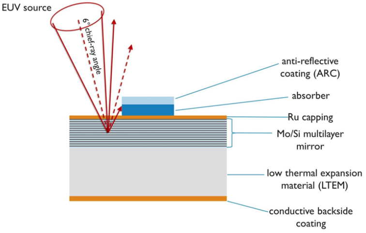
Fig. 2: Cross-section of an EUV mask. In EUV, light hits the mask at an angle of 6°. Source: Luong, V., Philipsen, V., Hendrickx, E., Opsomer, K., Detavernier, C., Laubis, C., Scholze, F., Heyns, M., “Ni-Al alloys as alternative EUV mask absorber,” Appl. Sci. (8), 521 (2018). (Imec, KU Leuven, Ghent University, PTB)
Wu: In general, for EUV we have several kinds of defects. The first one is phase defects. That one is mainly contributed from the substrate. After the multi-layer deposition step, the distortion will transfer to the top through the whole layer. That introduces phase defects. If people use optical inspection here, the sensitivity is around 50nm, 40nm or 30nm. If you use EUV for patterning at 18nm half-pitch, it looks like we still need a tighter spec for this kind of defect control. This defect is for the EUV mask blank. The other defects occur during the fabrication. That’s the regular or hard defects. For this one, because of the EUV patterns, the primary feature sizes are significantly smaller. It’s smaller than optical. For optical masks, the minimum main primary feature is around 80nm. But for EUV, it could be like 50nm and 40nm for the main primary feature. So that means the defect requirements are smaller. For this one, patterned mask inspection, compared with optical, is very challenging. The other kind of defect is something I call progressive defects. For progressive, we use the term haze. This defect is created during the usage or during the application. EUV is easy to have the defects from the wafer resist come to the mask even though they have a block layer and the pellicle. The EUV mask is easier to become contaminated during the application.
Levinson: You have a very small number of die on the reticle. It could be as few as one, but four or six is typical. So if you have four die on a mask and you get one killer defect, you lose 25% of your wafer yield for the whole fab. That’s a very significant effect just due to one particle. For a single die, you are completely in trouble. This imposes very stringent requirements on the mask.
SE: The good news is that defects on EUV mask blanks are down to single digit numbers. EUV mask blank demand is also strong, but prices are relatively high for these products. Any thoughts?
Levinson: We are in an industry where everybody will always try to drive the costs down. Back to the problems we were facing in trying to make EUV lithography cost effective, the cost of the mask blank itself was pretty far down on the list of concerns. It’s there, but not anywhere near as significant as other issues. For example, the exposure tools are expensive. The effective capital cost is quite significant unless you get adequate throughput. That’s a much bigger impact than the blank costs.
SE: EUV mask blanks are made by a blank supplier. Once the blank is made, it is shipped to a photomask vendor where the mask is made. To pattern the features on a photomask, mask makers use single-beam e-beam tools based on variable shaped beam (VSB) technology. Now, the industry has developed multi-beam mask writers. What does multi-beam bring to the party?
Fujimura: In general, multi-beam is thought to be required for EUV in any production use. You can do it with VSB, but it’s not practical for everyday use. The principal reason for it is if you want to write smaller features with EUV single patterns, and if you want to have SRAFs, the sizes of the features that you have to print on the mask are much smaller than what’s required today. That in turn requires a slower resist to be used. And it’s slow enough that regular VSB writers would have to do multiple passes of writing more than they usually do. They typically do two to four passes of writing. But it might become four to eight passes in order to avoid resist heating. That may become a problem. It’s principally because you need to write smaller features and that requires slower resists. People usually think of multi-beam as being needed because it’s independent of shot count. VSB writers are linear with shot count, while multi-beam writers are not. They are independent of shot count. But that’s not the reason why EUV masks need to be written with multi-beam. The majority of today’s deployment of EUV is done with very simple SRAFs. But even if you have simple SRAFs, like rectangular SRAFs only, there are still small dimensions. They need to be printed. For today’s very simple SRAF situation, we do not have a shot count problem. But we do have a slow resist problem. And for tomorrow’s EUV masks, where more sophisticated OPC and maybe even ILT (inverse lithography technology) is required to get the process window, you need it for both reasons.
SE: What about the data volumes for EUV masks?
Fujimura: There is a data volume issue for EUV masks once EUV masks are a regular event in the mask shop. For example, at the recent eBeam Initiative event, we talked about a lack of hierarchy. In EUV, every single mask is a full reticle mask as far as data preparation is concerned. For 193i, if you have 12 chips on a reticle, you can step and repeat them. You only describe it once. Then, in the job deck to the mask machine, you say, ‘Put this in 12 times.’ You can’t do that anymore when you are talking about EUV masks. EUV masks need to be corrected differently, depending on the feature’s relative location in the reticle. Being able to do one EUV mask is no problem. There are full reticle designs with 193i today. So you can handle it. But if you are talking about doing that for every mask, and you have a bunch of masks every day, now you have an infrastructure issue. OPC also takes a long time. If you just purely apply the lithography resolution, the OPC grid that you need to compute on would be twelve times bigger. It’s actually not that bad in real life because EUV resolution is not just limited by lithographic resolution like it was with 193i. But still, the resolution required to compute OPC/ILT is greater for EUV. The data infrastructure that is already an issue today will become even more of an issue once it’s being done all the time.
SE: Optical masks require a pellicle. A pellicle is a thin, transparent membrane that covers a photomask and prevents particles from falling on the mask. EUV lithography also requires a pellicle with a different structure. What are the challenges here?
Wu: We also talk a lot about the pellicle. The EUV pellicle, compared to the optical pellicle, is different. For the optical pellicle, the edge is sealed. We only have a few brief holes there. We also have a filter there. For EUV, we can’t use the optical pellicle structure.
Gallagher: We all assumed early on that there wasn’t going to be a pellicle. Because every material absorbs, the concept was you wouldn’t need a pellicle. You would just keep the scanner and the handling of the mask as clean as possible. Then, you don’t have to worry about the pellicle at all. So initially, any development of the pellicle didn’t start until much later. And then, the polysilicon pellicle was looked at by some very early, even in the 1980s and 1990s. That was abandoned. Then, the scanner made enormous progress on cleaning up the particles, but it wasn’t perfect. The logic makers said: ‘If I have one particle, I could be dead. I don’t want to take that risk. We need to come up with a pellicle if EUV is going to work.’ So if you look at all of the ranking problems, pellicles and mask defects are rising in the hierarchy of issues. Source power is becoming solved. Stochastics is still there. So now there is a pellicle, but its transmission is in the mid-80s percentile. It’s not incredibly robust. In addition, there are some reflections, so there is an extra membrane added. There is a loss of throughput. So there is a solution, but it would be nice if it was more transparent and robust. For high-volume manufacturing, when the power is getting even higher, real throughput is needed. So for a higher transmission, we are all looking for something else. Imec has a pellicle program. ASML has a program. Others talk about it. Our technology is based on carbon nanotubes. There are others out there.
Spence: Pellicles are needed for high-volume manufacturing. People are showing some solutions. There is a need for them. That will drive them to be developed.
SE: What’s the risk of running EUV lithography without the pellicle? Can’t we just clean the EUV mask on an intermittent basis?
Gallagher: Masks are expensive. There is a risk. You are printing wafers all the time. So who knows when the particle is going to fall on the mask. You run a huge amount of wafers at risk. Just cleaning the mask doesn’t help matters. Plus, you will limit the lifetime of the mask. You can’t clean it indefinitely.
Related Stories