
IP 뉴스
Challenges In Making And Testing STT-MRAM
2019.05.18 01:06
Next-gen memory offers speed of SRAM and unlimited endurance, but it’s not a simple technology to work with.
MAY 7TH, 2019 - BY: MARK LAPEDUS

Several chipmakers are ramping up a next-generation memory type called STT-MRAM, but there are still an assortment of manufacturing and test challenges for current and future devices.
STT-MRAM, or spin-transfer torque MRAM, is attractive and gaining steam because it combines the attributes of several conventional memory types in a single device. In the works for years, STT-MRAM features the speed of SRAM and the non-volatility of flash with unlimited endurance. STT-MRAM uses the magnetism of electron spin to provide non-volatile properties in chips.
But the technology is also complex, which is why it has taken longer than expected to ramp. STT-MRAM is shipping to a limited degree. Everspin is selling standalone STT-MRAM devices for solid-state storage drives (SSDs). Then, for some time, five chipmakers—GlobalFoundries, Intel, TSMC, Samsung and UMC—have been developing and/or ramping up an embedded version of STT-MRAM.
Still, chipmakers face some challenges in the fab to improve the current devices and scale them beyond 28nm or 22nm. In addition, test is playing a big role here. STT-MRAM requires new test equipment, which tests the magnetic field of the device. Then the device undergoes rigorous testing in various places in the flow, such as the fab, test floor and even post-test.
Even then, challenges remain. “The new and still to be solved part of MRAM testing is what happens when a MRAM chip is operating in a strong magnetic field,” said Dave Eggleston, a principal at Intuitive Cognition Consulting. “With non-magnetic devices, you don’t worry about this. With MRAM, it’s a new consideration. In general, it takes a strong magnetic field to disturb perpendicular STT-MRAM during operation. It’s something to verify, but certainly a solvable problem.”
So, the industry needs to pay close attention to STT-MRAM. “The landscape of embedded is at the point where customers are designing with the technology. We are now in that 18-month to two-year cycle with chips coming out with embedded MRAM,” Eggleston said.
What is MRAM?
MRAM, which is still a tiny market, was a $36 million business in 2017, according to Coughlin Associates and Objective Analysis. In total, the MRAM market is expected to reach $325 million by 2020, according to MKW Ventures Consulting.
STT-MRAM, phase-change memory (PCM) and resistive RAM (ReRAM) are among the new memory types in production today. Each technology is different and targeted for various applications.
Intel’s 3D XPoint technology is one example of PCM. PCM stores information in the amorphous and crystalline phases. ReRAM is based on the electronic switching of a resistor element.
STT-MRAM, which is different, is attractive for several reasons. “MRAM has a number of attractive attributes—it is fast (random reads and writes), non-volatile and low power, and offers low cost potential since the memory array can be embedded in the back-end interconnect layer of the chip with only three additional masks,” said Gill Lee, managing director of memory technology at Applied Materials, in a recent blog.
STT-MRAM consists of a one-transistor architecture with a magnetic tunnel junction (MTJ) memory cell, which serves as the storage element. “MRAM uses magnetic storage elements rather than conventional electric charges to store data. Each cell consists of two magnets: one that is stationary, and one that can flip. When the magnets are parallel to each other, resistance is low; when the second magnet flips and reverses direction, the resistance is high. Similar to PCM, the change in resistance correlates to a ‘0’ or ‘1’ data value,” explained Alex Yoon, senior technical director at Lam Research, in a blog.
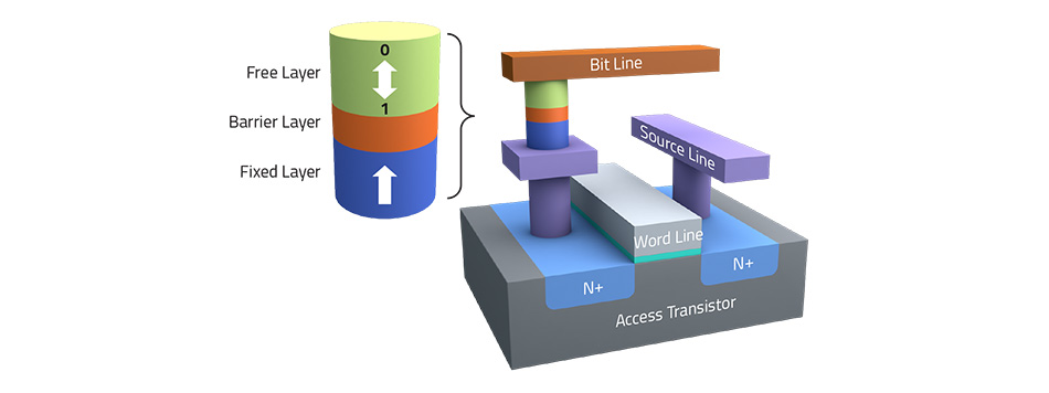
Fig. 1: MJT cell for STT-MRAM. Source: Lam Research
It’s a complex operation with several challenges. “MRAM has the characteristics of spin,” said Naoyoshi Watanabe, a senior engineer within the Memory Test System Planning Department at Advantest. “The electrons are rotating like a spin. It changes direction by an applied current. The timing of the change in direction has a quantum probability, depending on the angle of rotation.”
STT-MRAM is also prone to variations, which may cause some reliability issues. The big challenge for STT-MRAM is so-called “read disturb.” As you scale the cell, the read and write currents shrink and become too close with one another. This, in turn, may disturb the read cells during operation.
There are other issues. Today, the industry is developing MRAM based on 28nm or 22nm. “STT-MRAM is a technology certainly scalable from the 2xnm node down into the 1xnm node. Whether or not it can scale to 7nm or 5nm is still up for debate,” said Intuitive Cognition’s Eggleston.
Nonetheless, STT-MRAM is moving forward and targeted for two applications—embedded and standalone. Today, Everspin is the only company shipping standalone parts. It is shipping a 256Mbit part based on 40nm, while sampling a 28nm 1Gbit device.
The foundries are focusing on embedded MRAM, which is split into two categories—embedded flash replacement and cache. Typically, microcontrollers (MCUs) integrate several components on the same chip, such as a CPU, SRAM and embedded memory. Based on NOR flash, embedded flash memory (eFlash) is used for code storage.
The industry is ramping up 28nm MCUs with embedded NOR, with 16nm/14nm chips in R&D. But it’s difficult to scale embedded NOR at 28nm and beyond. It requires more expensive mask steps. “Many believe that 28nm/22nm will be the end of eFlash, not because of scalability limitations but because of economic barriers,” said David Hideo Uriu, product marketing director at UMC.
That’s where embedded STT-MRAM fits in. It is geared to replace embedded NOR at 28nm/22nm and beyond. STT-MRAM also can replace or augment the SRAM in an MCU, microprocessor or system-on-chip.
Automotive, IoT and other applications are among the growth drivers for MRAM. “UMC is preparing our 28nm/22nm technology with eMRAM as a platform base, which is scheduled to be ready in the second half of 2019,” Uriu said. “We believe MRAM is the next storage wave. The MRAM performance and low power coupled with persistence are the major reasons that MRAM is so flexible for many applications. For example, MRAM can be used in extreme-low-power designs, such as wearables, RFID-based applications like smart labels or trackers, as well as performance needs like edge and cloud applications. One example is data centers, where power is the highest portion of their operational costs.”
Uriu sees three apps for MRAM. “One is embedded MRAM. MRAM macros are embedded or integrated with MCUs. In addition, high-density MRAM is suitable for cache, acceleration of NAND flash, or as a replacement for SRAM applications,” he said. “Then, you have MRAM as a persistent DRAM replacement. This is for mission-critical enterprise applications, where power loss and lost memory can severely impact a client or for general power reduction.”
MRAM and other next-generation memory types also are being targeted for machine learning. Today’s systems with machine learning are using traditional memory, which consumes power. “It is estimated that a high percentage of power is used in simply moving data around, rather than actual computational functions. Any increase in performance can improve the machine learning functionality. Any lower power and persistence can dramatically save power versus current DRAM applications,” he added.
Making, testing MRAM
In the fab, meanwhile, MRAM involves the development of new materials, integration schemes and equipment. The process flow depends on whether it’s a standalone or embedded device.
For embedded, the process starts in a traditional fab, where a chipmaker fabricates a device. Then, the device is shipped to a separate fab facility called the backend-of-the-line (BEOL), where the metal layers and tiny copper interconnects are fabricated in chips.
In a device, the transistor resides on the bottom of the structure. The interconnects, which reside on the top of the transistor, consist of tiny copper wiring schemes that transfer electrical signals from one transistor to another. In the interconnect stack, logic chips have 9 to 12 metal layers. Each layer is connected to another layer with vias.
Chipmakers incorporate embedded STT-MRAM between the metal layers. For example, in Intel’s 22nm finFET technology, embedded MRAM is placed between metal 2 and metal 4 in the interconnect stack.
The STT-MRAM cell, dubbed the MTJ, consists of a dielectric tunnel barrier film based on magnesium oxide (MgO). The tunnel barrier (MgO) is sandwiched by two ferromagnetic layers based on a cobalt-iron-boron (CoFeB) compound. The CoFeB layer is 10 to 30 angstroms.
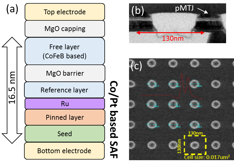
Fig. 2: (a) MTJ stack. (b) side view. (c) top view. Source: Applied Materials
To make an MTJ cell, the first step is to form a multi-layer stack of these materials on a bottom electrode using a deposition system. The film stack may have 20 to 30 layers. “Many metal and insulating layers need to be deposited using physical vapor deposition methods in pristine, sub-atmospheric, high vacuum conditions. Each layer must be precisely controlled and measured,” Applied Material’s Lee said.
Here’s where STT-MRAM is different than most devices—a test step is conducted after deposition. Using new and unconventional methods, a system applies a magnetic field to the stack to ensure the properties of the materials meet spec.
For this, one startup, Hprobe, is developing an MRAM blanket wafer tester. The system consists of a magnetic generator test head, which fits on a standard wafer prober. “The test is done after deposition of the MRAM stack of thin layers,” said Siamak Salimy, CTO of Hprobe. “This new magnetic generator can generate a perpendicular field above 2.5 Tesla and can run the hysteresis curve in less than 500ms.”
Hprobe’s system conducts measurements based on the magneto-optic Kerr effect. This involves the changes of light, which are reflected from a magnetized surface. Tesla, or T, represents the magnetic field strength of the system.
Following that step, the device follows a more traditional process flow, where the film stack is turned into an MTJ cell. The MTJ cell resembles a tiny nanopillar.
To make the nanopillar-like MTJ, a hardmask is applied on a portion on the stack. The other portions are etched using reactive ion etch tools or ion beam etch, or both. “The etch steps for MRAM devices are among the most challenging in the manufacturing process,” Lam’s Yoon said. “The cobalt-iron and cobalt-iron-boron magnetic layers are difficult to etch because they don’t readily form volatile compounds with plasma gases so they can be removed.”
More testing
Then, the final MTJ structure is encapsulated, forming a chip with embedded MRAM. From there, the device is sent to wafer sort in the test phase. Traditionally, in wafer sort, an electrical test is conducted on a die while it’s still on the wafer. Then, a device is packaged and tested using automatic test equipment (ATE).
The process flow is similar for STT-MRAM, but the test requirements are different for these devices. “In STT-MRAM testing, test technology is needed that supports error-bit analysis and its mode categorization on STT-MRAM chip measurements,” Advantest’s Watanabe said. “The error-bit mode can be identified by the switching current that flows through the MTJ during the write operation of STT-MRAM. However, it is difficult to measure the switching current because the switching occurs in the order of nanoseconds and the current is very low. Additionally, the real-time measurement of the switching is the challenge, since the switching is a probabilistic phenomenon based on quantum mechanics.”
Nonetheless, STT-MRAM undergoes several test steps. Besides the in-line fab flow, the device is tested on the test floor, including wafer probe and final test. Then there is a reliability test. This varies among chipmakers.
For wafer probe, STT-MRAM requires specialized equipment. Advantest and Hprobe are developing this type of test technology. For example, Hprobe has developed a different magnetic test head technology for the probe/parametric step. The test head, based on a magnetic generator, is also retrofitted on a prober. In simple terms, the system determines whether a device can withstand a magnetic field without becoming demagnetized.
“It’s a head that generates a magnetic field on top of the wafer. We do that at the same time, while probing the device. This alone extracts the hysteresis curve of the magnetic tunnel junction,” Hprobe’s Salimy said. “We are testing under a magnetic field. There are two physical parameters, which are related to the manufacturing process. These are called the coercivity field and thermal stability factor. The coercivity field is basically the amount of magnetic field that is needed to switch the spin of the device and bring the magnetic tunnel junction from a low level of resistance to a high level of resistance, or vice versa. The thermal stability factor is defined as the ratio of the energy barrier to switch the device from one state to another and the thermal energy at the operating temperature. It gives information on the data-retention performances of the memory point.”
Meanwhile, Advantest is working on several solutions in the arena, including a test module as well as a pair of magnetic field application test systems for wafer sort apps. The module, which works with a memory tester, measures subtle changes in resistance and the variation distribution of the current transition times during STT-MRAM switching operations. In addition, the company has developed a magnetic field test system using a prober, which is rated at ±800mT max@10mm.
In a separate system, it has devised a memory tester with a built-in electromagnet. With a magnetic field spec of 160mT, the electromagnet is connected to a wafer prober. “The following evaluations can be made with the magnetic field application system: 1) magnetic field resistance to external magnetic fields; 2) reliability evaluation by magnetic field assist instead of a voltage load; and 3) reduction of test time by memory cell 0/1 data inversion,” Advantest’s Watanabe said.
Wafer sort is only part of the solution. Assuming a device meets spec here, the chip then undergoes a final test step using standard ATE. For this, STT-MRAM is tested like any other memory device. The tester looks at several parameters, such as whether the bits will switch or not.
Typically, wafer probe and final test provide more than enough test coverage for conventional memories like DRAM and flash as well as most logic chips. That’s not enough for STT-MRAM, however. At one stage or another, chipmakers also conduct a form of reliability testing on the device. Obviously, the technology must be reliable if it’s used in automotive or other mission-critical apps.
For this, chipmakers are using custom equipment to test a sample. “That’s where they are taking a test chip with magnetic elements. You bring a magnet in close contact to the device and with a magnet of different strengths. Then they look at how many bits got disturbed through data retention. The variables are usually the strength of field, how close the magnet comes to bits themselves and the temperatures,” said Eggleston at Intuitive Cognition Consulting.
The goal is to solve a major issue. “The big unknown with MRAM is magnetic disturb,” Eggleston said. “In the case of eFlash or nonvolatile SRAM, we never worried about this. Now, reliability testing is done on chips, whether they are standalone or embedded. In this case you are exposing it to the possibility when it’s at the power-down state to see if you can disrupt the data retention or it could be during a write operation. What happens if you are writing the chip and there is a magnetic field? That’s a tricky one because you want to have a tough enough test, but you also want it to relate to the real world.”
For this step, the goal is to determine the magnetic field reliability specs for a given chip. Today, foundries are stating the spec, but this could change over time. “That’s still developing. Ultimately, there will be an industry reliability standard for magnetic fields, as well as static and dynamic fields, and how big those fields can be and at what temperatures. Temperatures have a big impact on MRAM disturb,” Eggleston said.
Still, the industry appears to be solving many of these and other issues. It’s only a matter of time before STT-MRAM reaches critical mass.
Now, in R&D, the industry is working on a future MRAM technology called spin-orbit torque MRAM (SOT-MRAM). It’s a faster version of STT-MRAM, but it’s still in its infancy. For now, though, the industry still needs to iron out the bugs in STT-MRAM.
Related Stories